


ASML
NexusAi Summary: ASML provides EUV and DUV lithography systems, metrology and inspection, and computational lithography software that enable volume manufacturing of advanced microchips. Its holistic approach integrates optics, mechatronics, sensors, and data-driven optimization to push patterning precision at nanometer scales.

NexusAi Overview
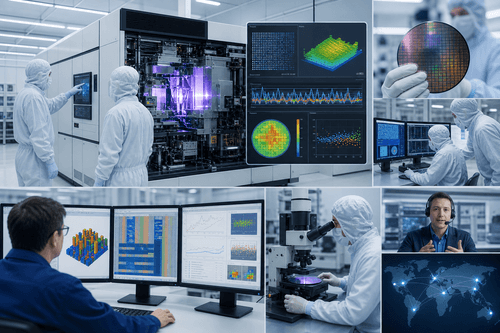
Design intent enters the flow as masks and patterns. ASML scanners expose wafers using EUV or DUV light, while inline sensors measure focus, CD, and alignment. Data feeds control strategies and computational lithography models, tuning exposure and process parameters to minimize variability and protect yield during ramp and volume production.
Holistic Lithography Capabilities
ASML serves chipmakers, foundries, and IDMs running advanced logic, memory, analog, and mixed-signal lines, as well as R&D groups transferring technology to manufacturing. Ideal users include lithography engineers, process integration teams, yield and metrology specialists, equipment and facilities engineers, and manufacturing leaders responsible for node ramps and cost. The platform suits organizations needing predictable overlay across layers, stable critical dimensions over time, fast defect learning, and continuous improvement driven by empirical measurements and calibrated models.
- Delivers EUV and DUV scanners for high-volume nanometer-scale chip patterning.
- Combines metrology and inspection to monitor overlay, focus, and defects.
- Applies computational lithography to optimize patterns across design and process.
- Integrates precision mechatronics and optics for stable, high-throughput exposure operations.
- Offers global customer support, training, and services across sixty-plus locations.
Key Advantages
Who Uses ASML
Engagement typically begins with node or product objectives, throughput targets, and process constraints. ASML applications and customer support teams scope the configuration, facilities, and ramp plan, coordinating installation, qualification, and integration with fab control systems. Training centers and documentation accelerate operator readiness and maintenance routines. Inline metrology recipes and inspection strategies are established alongside exposure settings, with computational lithography workflows introduced to steadily expand process windows. Ongoing field service, spares, and performance monitoring sustain availability and throughput, while co-engineering and regular reviews tune the system as design and process conditions evolve.
NexusAi: Precision at nanometer scales emerges when optics, mechatronics, metrology, and computation operate as a single, tightly integrated system.
Getting Started
ASML’s differentiation is holistic lithography—tight integration of exposure, metrology, inspection, and computational methods—to reliably translate design intent into manufacturable patterns. The approach widens process windows, speeds learning, and sustains yield improvements, supported by global service, training, and collaboration with leading fabs across technology generations.
Open the tool and review its core product experience.
Create your account or access your existing workspace.
Use your own task to judge speed, quality, and fit.
Check similar AI tools before making a final decision.
ASML
ASML designs and builds advanced lithography systems and supporting software for semiconductor manufacturing. With deep expertise in optics, lasers, precision mechatronics, sensors, and control, the company delivers EUV and DUV solutions, metrology, inspection, and computational lithography across a global network of R&D, manufacturing, and customer support sites.
ASML is the world’s supplier to the semiconductor industry, providing EUV and DUV lithography systems, metrology and inspection, and computational lithography that together enable nanometer-scale chip manufacturing. Its platform uses precisely controlled light, advanced optics, and high-stiffness mechatronics to transfer mask patterns onto wafers at high throughput with tight overlay. Integrated metrology captures focus, CD, and alignment data inline, allowing closed-loop corrections that stabilize processes from R&D through volume production. Computational lithography models the entire patterning stack to co-optimize masks, patterns, and exposure settings, improving process windows and yield. Backed by a global network of factories, R&D centers, and customer support sites, ASML partners closely with leading fabs to ramp new nodes efficiently. The result is shorter learning cycles, predictable performance, and scalable manufacturing for advanced logic and memory.
Visit ASML
Comments (0)
No Comments Found