


Siemens
NexusAi Summary: Siemens EDA is a comprehensive electronic design automation platform spanning IC, advanced packaging, and electronic systems. It combines AI-first methodologies, hardware-assisted verification, and cloud-delivered flows to accelerate design, improve manufacturability, and de-risk schedules at advanced nodes and 3D IC.

NexusAi Overview
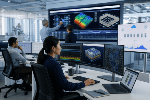
Teams plan architectures, co-design hardware and software, and prototype early while AI surfaces risks and optimizations. Verification scales from simulation to hardware-assisted platforms. Packaging and 3D IC analysis run alongside signoff and manufacturability checks, with cloud elasticity smoothing peak workloads and schedule crunches.
What It Does
Best for semiconductor companies, system OEMs, hyperscalers, and startups building complex SoCs, chiplets, or electronics-rich products. Ideal users include design and verification engineers, physical implementation leads, packaging specialists, CAD and methodology teams, and program managers seeking predictable schedules, earlier risk discovery, and coordinated cross-discipline collaboration.
- AI guided verification accelerates defect discovery and coverage closure across flows.
- 3D IC planning and analysis mitigate thermal hotspots and interposer complexity.
- Hardware software co design enables shift left optimization before silicon commitments.
- Advanced node readiness streamlines three nanometer and two nanometer design challenges.
- Cloud managed EDA deployments scale compute elastically for peak verification workloads.
Why It Matters
Who Benefits
Begin by aligning target technologies, foundry enablement, and project objectives with Siemens EDA solutions. Deploy in your cloud or data center, then enable workloads for simulation, emulation, implementation, packaging, and signoff. Siemens EDA consulting accelerates methodology setup, while ecosystem integration streamlines partner and foundry collaboration. Upskill teams through Siemens Xcelerator Academy training paths tailored to IC, packaging, and verification disciplines. Scale compute elastically for peaks and codify best practices in reference flows to achieve predictable schedules and quality outcomes.
NexusAi: Shift-left, AI-first EDA turns exponential complexity into predictable, verifiable, manufacturable outcomes.
Getting Started
Siemens EDA stands out by embedding AI across the workflow, validating complex architectures with hardware assistance, and operationalizing 3D IC and advanced-node delivery. With cloud elasticity, ecosystem alignment, and expert services, it transforms rising complexity into predictable schedules, manufacturable designs, and faster time-to-market.
Open the tool and review its core product experience.
Create your account or access your existing workspace.
Use your own task to judge speed, quality, and fit.
Check similar AI tools before making a final decision.
Siemens
Siemens EDA, part of Siemens Digital Industries Software, advances electronic design automation across ICs and electronic systems. The team combines deep methodology expertise with AI-first approaches, digital twin thinking, and hardware-assisted verification to help organizations deliver reliable, manufacturable products at scale.
Siemens EDA delivers an end-to-end portfolio for IC and electronic systems design, verification, and manufacturing. Built around an AI-first methodology and digital twin thinking, it helps teams move from reactive debug to predictive engineering. Hardware-assisted verification validates complex architectures—demonstrated on Arm AGI CPU—while cloud-delivered EDA scales compute for peak regression and signoff bursts. The platform addresses the industry’s convergence of exponential complexity, rising costs, and constrained talent by unifying implementation, verification, packaging, and manufacturing readiness. 3D IC and heterogeneous integration are supported with planning, analysis, and verification that account for thermal, interconnect, and test challenges. Shift-left verification augments coverage and yield prediction using intelligent pattern recognition. Advanced-node readiness supports aggressive technology transitions, while ecosystem integration aligns tools, partners, and foundry collaboration. Backed by consulting services and Siemens Xcelerator Academy, organizations can upskill quickly and deploy robust, production-grade flows.
Visit Siemens
Comments (0)
No Comments Found