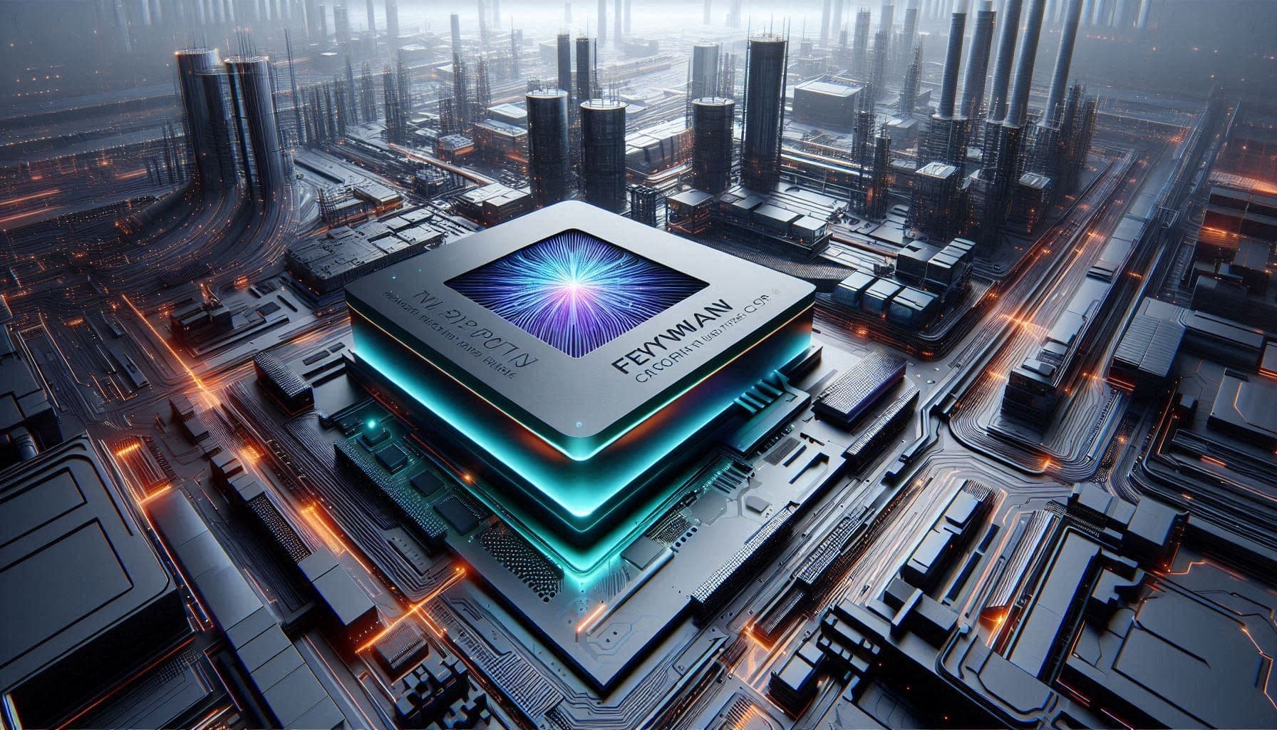
NVIDIA’s rumored Feynman AI chip and TSMC’s CoPoS packaging roadmap show why the next AI infrastructure race may be won through advanced packaging, not only faster GPUs.
NVIDIA’s future Feynman AI chip is still an analyst-driven and supply-chain-reported story, not a fully announced product. But the direction is important: future AI accelerators are becoming so large and complex that traditional advanced packaging approaches may hit economic and physical limits. That is why TSMC’s CoPoS roadmap is attracting attention.
For years, CoWoS has been one of the key packaging technologies behind high-end AI chips. It allows logic chiplets, high-bandwidth memory and interconnect layers to work together in one package. But AI models are growing, memory bandwidth requirements are rising, and hyperscalers want more compute per system. At some point, package size, interconnect density, thermal design and cost become just as strategic as the GPU architecture itself.
CoPoS, or Chip-on-Panel-on-Substrate, is important because it points toward larger panel-based packaging that could support ultra-large AI accelerators. If NVIDIA Feynman becomes one of the first major adopters, it would signal that the AI chip race is entering a new phase where advanced packaging becomes a headline technology category, not just a back-end manufacturing detail.
Why AI chips are outgrowing traditional packaging
Modern AI accelerators are no longer simple single-die processors. They combine GPU compute, HBM memory, chiplets, interposers, substrates, power delivery, cooling requirements and high-speed interconnects. The goal is to move data between compute and memory as quickly and efficiently as possible, because AI training and inference are limited by bandwidth as much as raw compute.
As model sizes and inference workloads grow, the package around the chip becomes a performance bottleneck. More memory, wider interconnects and larger compute fabrics require more physical area. This is why packaging technologies such as CoWoS, CoWoS-L, CoWoS-R and future CoPoS matter for AI infrastructure.
What CoPoS could change for NVIDIA Feynman
The reported attraction of CoPoS is scale. Panel-based packaging may allow TSMC to build larger AI chip packages than conventional wafer-level approaches can economically support. That could help future accelerators integrate more compute dies, memory stacks and supporting components into a single high-performance package.
For NVIDIA, this could matter if Feynman targets a major step beyond today’s AI accelerator package sizes. A larger package could support more HBM capacity, higher bandwidth, wider chiplet layouts and new system-level architectures. The practical outcome would be more powerful AI compute nodes for training, inference, reasoning models and agentic workloads.
The CoPoS supply chain is becoming a new battlefield
TrendForce’s report that TSMC is running dual-track equipment evaluation is important because CoPoS is not only a technology transition. It is also a supply-chain transition. Panel-level packaging requires different equipment, materials, process control and vendor coordination from mature wafer-level packaging.
This could create opportunities for global equipment vendors, local Taiwanese suppliers, substrate makers, glass-related material providers, ABF suppliers, inspection systems and advanced packaging specialists. As AI chip demand rises, the companies that control packaging capacity may become just as strategically important as those that design the processors.
Why this matters for AI tools and model users
At first glance, CoPoS sounds far removed from everyday AI tools. But every AI assistant, coding agent, video model, research agent, enterprise copilot and local AI workflow depends on the hardware supply chain underneath it. If packaging capacity is constrained, AI compute remains expensive and limited. If packaging improves, larger and more efficient AI systems become possible.
This is especially important for frontier models and enterprise AI. More capable reasoning models, multimodal systems and autonomous agents require more compute, more memory and better energy efficiency. Packaging breakthroughs can indirectly shape which AI tools become affordable, fast and widely available.
The key risk is timing and manufacturing maturity
CoPoS should not be treated as a solved upgrade path yet. Panel-level packaging has to prove yield, reliability, thermal performance, substrate stability, equipment maturity and cost efficiency at scale. A promising roadmap does not automatically mean mass production will ramp smoothly.
NexusAI users should watch three signals: whether TSMC confirms production timelines, whether NVIDIA officially reveals Feynman packaging details, and whether CoPoS demonstrates better economics for ultra-large AI packages. Until then, the safest interpretation is that CoPoS is a strategically important packaging direction with major upside, but still dependent on manufacturing execution.